Printed Circuit Boards
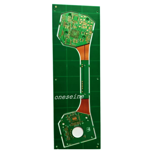
14 Layer Industrial Control Soft Hard Combination Flex PCB Board Thickness
- flex pcb manufacturer
- rigid flex pcb
- quick turn flex pcb
- semi flex pcb
- Product description: flex circuit materials kapton flex circuit bendable pcb flex pcb quote flex circuit assembly flex coverlay quick turn flex pcb stiffener flex pcb custom flex pcb flexible pcb printing flex p
14 Layer Industrial Control Soft Hard Combination Flex PCB Board Thickness
PCB product Introduction
Application field: High end industrial control field
Material: DuPont+Shengyi S1000-2M
Number of layers: 14
Plate thickness: 2.0 ± 0.2mm
Minimum aperture: laser hole 0.1mm, mechanical hole 0.2mm,
Minimum line width/line spacing: 0.076mm
Copper thickness: 1OZ each on the inner and outer layers
Solder resistance: green oil with white lettering and yellow film
Surface technology: sinking gold
Product features: BGA pad 0.2mm, resin plug holes are required for the holes in the BGA pad
The 14 layer industrial control soft and hard bonding board is one of the series of soft and hard bonding boards developed and produced by ONESEINE. It is produced using DuPont+Shengyi S1000-2M material mixed pressing and surface gold sinking processes, and adopts laser drilling method, with a minimum of 0.1mm. This PCB circuit board is widely used in the field of industrial control.
The thickness of a flexible (flex) PCB is an important design consideration that can vary depending on the specific requirements of the application. Here are some key points to understand about flex PCB thickness:
1. Standard Flex PCB Thicknesses:
- Flex PCBs typically range in thickness from 0.05 mm (2 mils) to 0.5 mm (20 mils), with the most common thicknesses being 0.1 mm (4 mils), 0.2 mm (8 mils), and 0.3 mm (12 mils).
- The choice of thickness depends on factors such as the required flexibility, the number of copper layers, the need for stiffeners, and the overall space constraints.
2. Single-layer vs. Multi-layer Flex PCBs:
- Single-layer flex PCBs are typically thinner, ranging from 0.05 mm to 0.1 mm, as they only have a single copper layer.
- Multi-layer flex PCBs, which can have 2, 4, 6, or more copper layers, are generally thicker, ranging from 0.1 mm to 0.5 mm, depending on the number of layers.
3. Considerations for Flex PCB Thickness:
- Flexibility: Thinner flex PCBs (0.05 mm to 0.2 mm) are more flexible and can withstand a higher degree of bending, making them suitable for applications that require frequent flexing or folding.
- Rigidity: Thicker flex PCBs (0.3 mm to 0.5 mm) provide more rigidity and stability, which can be beneficial for applications where the flex PCB needs to maintain its shape or support heavier components.
- Space Constraints: The overall thickness of the flex PCB must fit within the available space in the final assembly, which may dictate the choice of thickness.
- Copper Layers: The number of copper layers in a flex PCB directly impacts the overall thickness, with more layers adding to the overall thickness.
- Stiffeners: The use of stiffeners, which are rigid sections added to the flex PCB, can also contribute to the overall thickness.
4. Customized Flex PCB Thickness:
- In some cases, custom or specialized flex PCB thicknesses may be required to meet the unique requirements of an application.
- Manufacturers may be able to accommodate custom thickness requirements, but this may come with additional costs and lead times.
When choosing the appropriate flex PCB thickness, it is essential to consider the specific design requirements, the flexibility needs, the component placement, and the overall space constraints of the application. Consulting with a flex PCB manufacturer can help determine the most suitable thickness for your project.
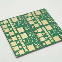
The flex PCB stack-up refers to the layered structure of a flexible printed circuit board, including the materials and their arrangement. The stack-up design is crucial for ensuring the performance, reliability, and manufacturability of the flex PCB. Here are the key aspects to consider when designing the flex PCB stack-up:
1. Copper Layers:
- The number of copper layers in a flex PCB can range from 1 (single-layer) to 8 or more (multi-layer).
- The copper layer configuration, such as the number of signal, ground, and power layers, depends on the electrical and functional requirements of the design.
2. Dielectric Layers:
- The dielectric layers in a flex PCB are typically made of polyimide, polyester, or other flexible insulating materials.
- The thickness and properties of the dielectric layers impact the flex PCB's mechanical flexibility, electrical performance, and reliability.
3. Cover Layers:
- Cover layers, also known as "coverlay" or "solder mask," are protective layers applied to the top and bottom surfaces of the flex PCB.
- These layers provide protection against environmental factors, such as moisture, dust, and physical damage, and can also help with surface finishes.
4. Stiffeners:
- Stiffeners are rigid sections or reinforcements added to the flex PCB, typically in specific areas where additional support is required.
- Stiffeners can be made of materials like FR-4, polyimide, or metal, and are used to improve the overall rigidity and stability of the flex PCB.
5. Adhesives:
- Adhesives are used to bond the various layers of the flex PCB together, ensuring structural integrity and reliable layer-to-layer interconnections.
- The type and thickness of the adhesives can impact the flex PCB's flexibility, thermal performance, and reliability.
6. Surface Finishes:
- The surface finishes, such as ENIG (Electroless Nickel Immersion Gold) or HASL (Hot Air Solder Leveling), are applied to the copper layers to protect them and facilitate soldering.
- The choice of surface finish can also affect the flex PCB's electrical and mechanical properties.


Categories
Latest News
Contact Us
Contact: Ms Tracy
Phone: 0086 18682010757
Tel: 0086 18682010757
Add: Building9,Xinyuan Industrial Park,Tangwei,Fuyong,Baoan,Shenzhen,China
 Tracy
Tracy