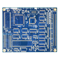
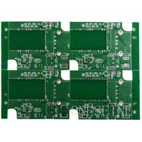
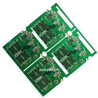
Fr4 PCB
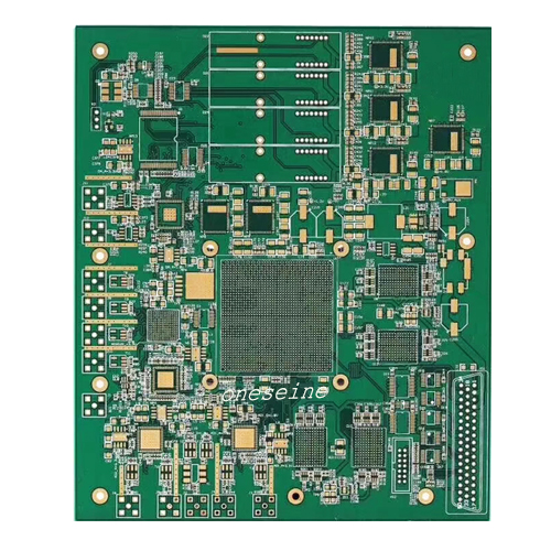
BGA FR4 Circuit Board For Data Acquisition Card PCB Manufacturing Companies Near Me
- 8Layer
- fr4 PCB
- Green pcb
- DAQ PCB
- Product description: quick pcb prototyping small pcb manufacturer cheap pcb prototype uk pcb order china pcb manufacturing companies near me custom flex pcb pcb making company best prototype pcb manufacturer get p
BGA FR4 Circuit Board For Data Acquisition Card PCB Manufacturing Companies Near Me
PCB parameter:
PCB material:FR4
Board size:15*18cm
Surface finish:ENIG
Copper weight:1OZ
Solder mask:Green
Silkscreen:White
Optimizing the layout and routing of a DAQ card PCB to minimize noise and interference is an important aspect of the design process. Here are some key recommendations:
1. Separate Analog and Digital Sections:
- Physically separate the analog and digital sections of the PCB to reduce cross-talk and electromagnetic interference (EMI) between the two.
- Route the analog and digital traces on different PCB layers, if possible, to provide additional isolation.
2. Ground Plane Considerations:
- Use a continuous ground plane on at least one layer of the PCB to provide a low-impedance return path for the signals.
- Ensure the ground plane is free of breaks, slots, or other discontinuities that can create ground loops and degrade signal integrity.
- Connect all ground points on the PCB to the ground plane using short, low-impedance traces.
3. Signal Routing:
- Route analog and digital traces on separate layers to minimize coupling.
- Keep analog and digital signal traces as short as possible to reduce noise pick-up.
- Route traces perpendicular to each other (e.g., analog traces perpendicular to digital traces) to minimize cross-coupling.
- Use controlled impedance traces for high-speed digital signals to avoid reflections and maintain signal integrity.
4. Decoupling Capacitors:
- Place decoupling capacitors close to the power pins of each IC to provide local high-frequency bypassing.
- Select capacitors with appropriate values and low equivalent series resistance (ESR) to effectively filter out high-frequency noise.
5. Power Supply Considerations:
- Provide separate power planes or traces for analog and digital sections to minimize cross-talk.
- Use ferrite beads or LC filters on the power supply lines to filter out high-frequency noise.
- Ensure the power supply is well-regulated and has low noise to avoid introducing noise into the analog signals.
6. Shielding and Isolation:
- Consider adding a ground plane or shielding layer around the analog section of the PCB to isolate it from the digital section.
- Use guard traces or grounded copper pours around sensitive analog traces to provide additional shielding.
- Carefully plan the placement of connectors and cable routing to minimize the introduction of external noise sources.
7. Thermal Management:
- Ensure the layout and routing allow for effective heat dissipation, especially for high-power components.
- Consider the use of thermal vias and heat sinks to improve thermal management.
By following these recommendations, you can optimize the layout and routing of a DAQ card PCB to minimize noise and interference, ensuring reliable and accurate data acquisition.
I'd be happy to provide some information about data acquisition card PCBs.
A data acquisition (DAQ) card is a printed circuit board (PCB) that is used to interface a computer with the external world, allowing it to measure and control physical quantities such as voltage, current, temperature, pressure, and more.
The key components typically found on a DAQ card PCB include:
1. Analog-to-Digital Converter (ADC): The ADC is responsible for converting analog input signals into digital values that can be processed by the computer.
2. Digital-to-Analog Converter (DAC): The DAC is used to convert digital values from the computer into analog output signals.
3. Multiplexer: The multiplexer allows the DAQ card to read multiple analog input channels by connecting them one at a time to the ADC.
4. Signal Conditioning Circuitry: This circuitry ensures that the input signals are within the appropriate voltage range and noise levels for the ADC.
5. Microcontroller or FPGA: The on-board microcontroller or FPGA is responsible for controlling the operation of the DAQ card, handling data transfers, and communicating with the host computer.
6. Connectors: The PCB typically includes one or more connectors, such as BNC, screw terminals, or D-Sub, to interface with the external sensors and devices.
7. Power Circuitry: The power circuitry provides the necessary voltage supplies for the various components on the DAQ card.
The design of a DAQ card PCB involves careful consideration of factors such as signal integrity, electromagnetic interference (EMI), and thermal management to ensure reliable and accurate data acquisition. The layout and routing of the traces on the PCB, as well as the selection of appropriate components, are critical to the performance of the DAQ card.
If you have any specific questions about the design or implementation of a DAQ card PCB, feel free to ask, and I'll do my best to provide a helpful response.
Categories
Latest News
Contact Us
Contact: Ms Tracy
Phone: 0086 18682010757
Tel: 0086 18682010757
Add: Building9,Xinyuan Industrial Park,Tangwei,Fuyong,Baoan,Shenzhen,China
 Tracy
Tracy