Fr4 PCB
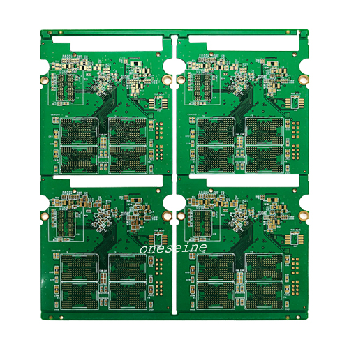
Six Layer PCB Material Fr4 Solid-state Drive Circuit Board Manufacture
- nanya fr4 material
- material fr 4
- multilayer pcb
- enig pcb
- Product description: fr4 ul 94 v0 fr5 pcb glass epoxy fr4 pcb ipc 4101 fr4 isola fr4 jlcpcb fr4 ltcc pcb material fr 4 mcigicm fr 4 copper clad pcb laminate circuit board nanya fr4 nema fr4 pcb board material f
Six Layer PCB Material Fr4 Solid-state Drive Circuit Board Manufacture
Number of layers: 6
Material: FR-4
Plate thickness: 1.6mm
Surface treatment: imersion gold
Minimum aperture: 0.2mm
Outer line width/line spacing: 4/4mil
Inner line width/line spacing: 3.5/4.5mil
Application area: Solid State Drive
Here are some key points about a 6-layer solid-state drive (SSD) PCB circuit board:
Layer Structure:
- The 6-layer PCB structure typically consists of:
1. Top Copper Layer
2. Inner Layer 1 (Ground Plane)
3. Inner Layer 2 (Signal Routing)
4. Inner Layer 3 (Power Plane)
5. Inner Layer 4 (Signal Routing)
6. Bottom Copper Layer
Design Considerations:
- The multiple copper layers provide improved power distribution, ground planes, and signal routing capabilities compared to fewer layer PCBs.
- The power and ground planes help with power delivery, noise reduction, and EMI/EMC performance.
- Careful signal routing on the inner signal layers helps maintain signal integrity for high-speed interfaces.
- Vias are used to interconnect the different copper layers as needed.
- Component placement and trace lengths are optimized for performance.
Applications:
- 6-layer PCBs are common in high-performance SSD designs to handle the bandwidth and power requirements.
- They are used in enterprise-class, client, and consumer-grade SSDs from leading manufacturers.
- The multilayer structure provides the necessary layout flexibility and electrical characteristics for SSD controllers, NAND flash, DRAM, and other supporting components.
Advantages:
- Improved power distribution and ground integrity
- Better signal integrity for high-speed interfaces
- Compact, dense layout for small form factor SSDs
- Scalable design for different SSD capacity and performance tiers
Does this help summarize the key aspects of a 6-layer SSD PCB circuit board? Let me know if you need any clarification or have additional questions.
How do the power and ground planes in a 6-layer SSD PCB help with thermal management?
The power and ground planes in a 6-layer SSD PCB design play an important role in thermal management:
1. Power Plane Distribution:
- The dedicated power plane(s) provide low-impedance distribution of power to all the components on the SSD.
- This efficient power delivery helps minimize voltage drops and reduces I²R heating in the traces.
- The wide copper planes can act as heat spreaders, transferring heat from hot spots to cooler areas of the board.
2. Ground Plane Thermal Conduction:
- The continuous ground plane(s) serve as a thermal sink, drawing heat away from components.
- Heat generated by the SSD controller, NAND flash, DRAM, and other ICs can be efficiently conducted into the ground plane.
- The ground plane acts as a large heat spreader, distributing the thermal energy across the entire PCB area.
3. Thermal Vias:
- Thermal vias are used to connect the top/bottom copper layers to the internal ground and power planes.
- These vias help transfer heat vertically through the PCB layers, improving overall thermal dissipation.
- Strategically placing thermal vias under high-power components enhances local heat removal.
4. Heatsink Integration:
- The ground and power planes provide a low-resistance thermal path to the PCB edges.
- This allows for effective integration of heatsinks or other cooling solutions onto the SSD assembly.
- The thermal energy from the components can be efficiently transferred to the heatsink for dissipation.
By leveraging the power and ground planes, the 6-layer SSD PCB design optimizes thermal management and helps maintain the performance and reliability of the SSD under various operating conditions. The multilayer construction provides the necessary thermal pathways for effective heat dissipation.
What are some design considerations for optimizing the thermal management of the 6-layer SSD PCB?
There are several key design considerations for optimizing the thermal management of a 6-layer SSD PCB:
1. Component Placement and Spacing:
- Carefully plan the placement of high-power components like the SSD controller, NAND flash, and DRAM.
- Locate these components in close proximity to allow for efficient heat transfer between them.
- Maintain adequate spacing between components to prevent hot spots and allow for airflow.
2. Thermal Vias:
- Strategically place thermal vias under and around high-power components.
- Use an optimized via pattern and density to provide low-resistance thermal paths to the ground and power planes.
- Consider using larger diameter vias (e.g., 0.3-0.5 mm) to improve thermal conductivity.
3. Ground and Power Plane Design:
- Maximize the copper area of the ground and power planes to enhance thermal spreading.
- Avoid large cutouts or openings in the planes that could disrupt the thermal conduction.
- Ensure the planes have sufficient thickness (e.g., 2-4 oz copper) for effective heat transfer.
4. Heatsink Integration:
- Design the PCB layout to facilitate easy integration of heatsinks or other cooling solutions.
- Provide ample copper area at the PCB edges for secure heatsink attachment.
- Consider adding thermal pads or thermal interface material (TIM) between the PCB and heatsink.
5. Airflow Optimization:
- Analyze the airflow patterns around the SSD assembly and optimize component placement.
- Use strategically located vents or cutouts in the PCB to promote air circulation.
- Coordinate the PCB design with the enclosure or system-level thermal management.
6. Thermal Simulation and Analysis:
- Perform detailed thermal simulations using computational fluid dynamics (CFD) tools.
- Analyze the heat dissipation, temperature distribution, and potential hot spots on the PCB.
- Use the simulation results to refine the component placement, via design, and other thermal management strategies.
By addressing these design considerations, the 6-layer SSD PCB can be optimized for effective thermal management, ensuring reliable operation and maintaining the performance of the SSD under various operating conditions.
Categories
Latest News
Contact Us
Contact: Ms Tracy
Phone: 0086 18682010757
Tel: 0086 18682010757
Add: Building9,Xinyuan Industrial Park,Tangwei,Fuyong,Baoan,Shenzhen,China
 Tracy
Tracy