News
PCB design software Altium Designer vias (through holes, blind vias and buried vias)
PCB design software Altium Designer vias (through holes, blind vias and buried vias)
Today's electronic components are increasingly trending toward miniaturization and high-density design. The most obvious benefit of these is the saving of energy. In some ways, it also brings more design space to engineers, but there are joys and sorrows. Miniaturized design requires high production processes and increased technical difficulty, and in terms of engineer design, sometimes too little space introduces some trouble. Especially when designing PCB boards, PCB wiring has become a difficult problem because more and more components are packaged in BGA. In order to solve the problem of PCB routing, blind holes and buried holes have appeared in the PCB board production process.
Before talking about Blind vias and Buried vias, let's recall the vias on the PCB, which is the way we use the most common PCB layer to layer. In fact, the hole we often say is the through hole. Let's take a picture of the difference between them.
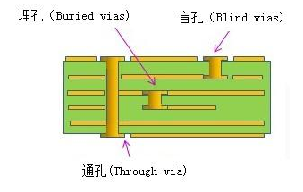
The appearance of blind holes and buried holes gives engineers more design space, because the layers that they do not go, engineers can use other lines. Of course, these designs are generally used only when they are necessary. Because blind holes and buried holes will increase the manufacturing cost of PCBs, and the maintenance inspection will increase the difficulty. Therefore, it is not necessary to use blind holes and buried holes. The way.
Well, let's talk about the introduction of vias. Let's take a look at how PCB design software (here Altium Designer 18 is used as an example software) is done.
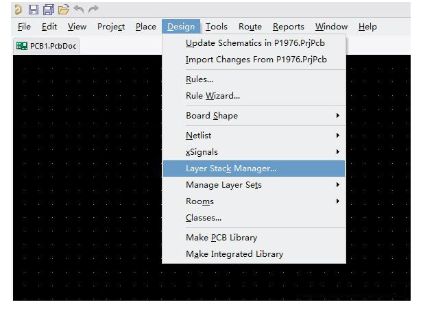
As shown above: Design=>Layer Stack Manager... (or press the shortcut key DK), the following interface will appear:
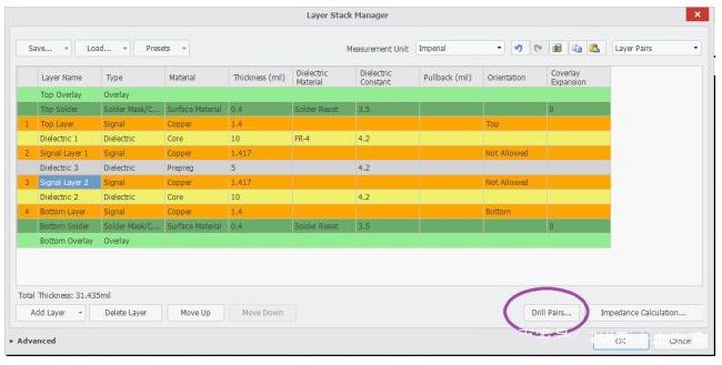
Click on the (Drill Pairs...) in the circle and the following image will appear:
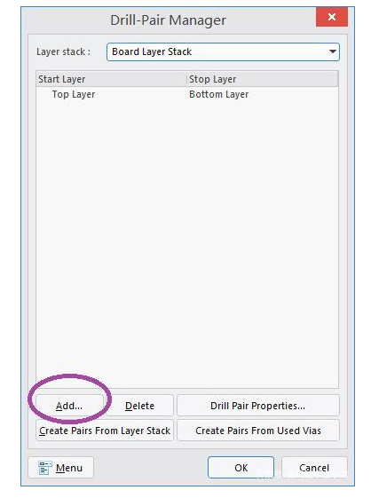
At this point, it is very clear. We can see that the default via is actually a via. It is the Start Layer to the Stop Layer. It corresponds to the Top Layer to the Bottom Layer. ). Now let's add Add... (circle in the figure) to add blind holes or buried holes. After clicking, the following picture appears:
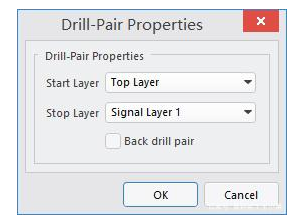
When you get to this dialog box, it is very intuitive. If you select Top Layer to Singnal Layer 1, it corresponds to the previous picture. Obviously, this is the so-called blind hole. We add it first, that is, click OK. In the same way, add buried holes, ie Singnal Layer 1 to Singnal Layer 2, and click OK. Then the following picture will appear:
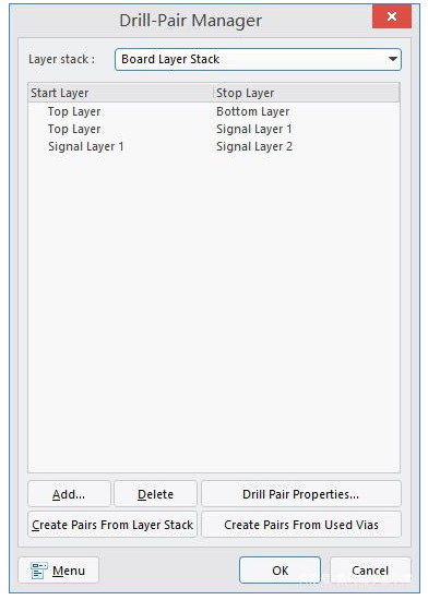
This is the type of via we added. The work is almost complete, you can click OK to exit to the PCB design interface step by step. On the PCB design interface, we place three vias, from top to bottom, and then click each via separately. Clicking on the via will bring up the dialog on the right as shown below:
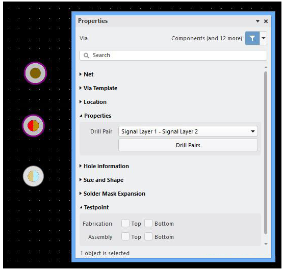
We select the type of via we just set in the Drill Pair in Properties. From top to bottom, the first one is the through hole, the top layer to the bottom layer (Bottom Layer), and the second one is the blind hole. That is, Top Layer to Singnal Layer 1, the third is buried hole, that is, Singnal Layer 1 to Singnal Layer 2. The relationship between the initial layer and the end layer of the via hole can also be seen very clearly from the internal color of the via.
Ok, let's learn about the vias of the PCB. Did you learn this?
Categories
Latest News
Contact Us
Contact: Ms Tracy
Phone: 0086 18682010757
Tel: 0086 18682010757
Add: Building9,Xinyuan Industrial Park,Tangwei,Fuyong,Baoan,Shenzhen,China
 Tracy
Tracy