News
How should the dielectric constant of PCB board material be measured at millimeter wave frequency?
How should the dielectric constant of PCB board material be measured at millimeter wave frequency?The dielectric constant (Dk) or relative dielectric constant of a PCB board material is not a constant constant – although it is a constant from its naming. For example, the Dk of a material changes with frequency. Similarly, if different Dk test methods are used on the same piece of material, different Dk values may be measured, even if they are all accurate. As circuit board materials are increasingly used in millimeter-wave frequencies, such as 5G and advanced driver assistance systems, it is important to understand the changes in Dk with frequency and which Dk test method is "appropriate".
Although organizations such as IEEE and IPC have dedicated committees to explore this issue, there is currently no standard industry test method to measure the Dk of board materials at millimeter wave frequencies. This is not because of the lack of measurement methods. In fact, a reference paper published by Chen et al.1 et al. describes more than 80 methods for testing Dk. However, no single method is ideal, and each method has its advantages and disadvantages, especially in the frequency range of 30 to 300 GHz.
Circuit test vs raw material test
There are generally two broad categories of test methods used to determine the Dk or Df (loss tangent or tan δ) of the board material: raw material measurements, or measurements made in circuits made of materials. Raw material-based testing relies on high-quality, reliable test fixtures and equipment to directly test raw materials to obtain Dk and Df values. Circuit-based testing typically uses common circuits and extracts material parameters from circuit performance, such as measuring the center frequency or frequency response of a resonator. Raw material testing methods often introduce uncertainties associated with test fixtures or test fixtures, and circuit test methods involve uncertainty from test circuit design and processing techniques. Because of the difference between the two methods, the measurement results and accuracy levels are usually inconsistent.
For example, the X-band clamped stripline test method defined by IPC is a test method for raw materials, and the results cannot be consistent with the Dk results of circuit tests of the same material. Clamped stripline raw material testing method is to build a stripline resonator by clamping two pieces of material to be tested (MUT) in a special test fixture. There is air between the material to be tested (MUT) and the thin resonator circuit in the test fixture, and the presence of air reduces the measured Dk. If the circuit test is performed on the same board material, and the air is not entrained, the measured Dk is different. For high frequency circuit board materials with a Dk tolerance of ±0.050 as determined by raw material testing, the circuit test will achieve a tolerance of approximately ±0.075.
The board material is anisotropic and typically has different Dk values on three material axes. The Dk value typically differs very little between the x-axis and the y-axis, so for most high frequency materials, Dk anisotropy generally refers to a Dk comparison between the z-axis and the x-y plane. Due to the anisotropy of the material, the Dk of the measured z-axis is different from the Dk of the xy plane for the same material to be tested (MUT), although the values of the Dk obtained by the test method and the test are all "correct". .
The type of circuit used for circuit testing also affects the value of the Dk being measured. Typically, two types of test circuits are used: a resonant structure and a transmission/reflection structure. Resonant structures typically provide narrowband results, while transmission/reflection tests are often broadband results. The method of using a resonant structure is generally more accurate.
Test method example
A typical example of raw material testing is the X-band clamped stripline method. It has been used by high frequency board manufacturers for many years and is a reliable means of determining Dk and Df (tan δ) in the z-axis of board materials. It uses a clamped clamp to form a sample of the material to be tested (MUT) into a loosely coupled stripline resonator. The measured quality factor (Q) of the resonator is no-load Q, so cable, connector and fixture calibration have little effect on the final measurement. The copper clad circuit board needs to etch away all the copper foil before testing, and only test the dielectric raw material substrate. The circuit raw materials are cut to a certain size under certain environmental conditions and placed in fixtures on both sides of the resonator circuit (see Figure 1).
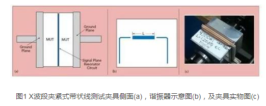
The resonator design is a half-wavelength resonator with a frequency of 2.5 GHz, so the fourth resonant frequency is 10 GHz, which is the resonance point commonly used for Dk and Df measurements. Lower resonant and resonant frequencies can be used – even higher fifth resonant frequencies can be used, but higher resonant points are often avoided because of the effects of harmonics and stray waves. Measuring extraction of Dk or relative dielectric constant (εr) is simple:

Where n is the first resonant frequency, c is the speed of light in free space, fr is the center frequency of the resonance, and ΔL compensates for the electrical length extension caused by the electric field in the coupling gap. It is also simple to extract tan δ(Df) from the measurement, which is the 3dB bandwidth-dependent loss of the resonance peak minus the conductor loss (1 / Qc) of the resonator circuit.
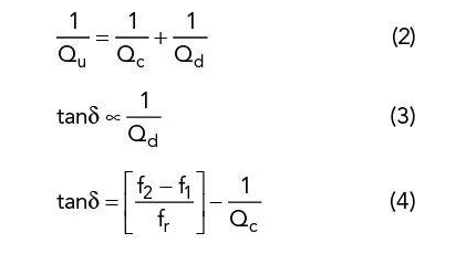
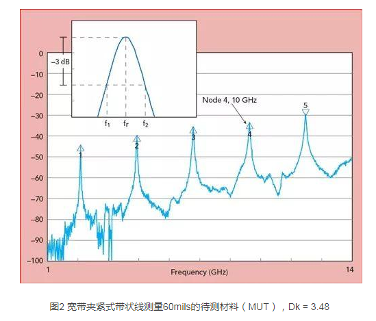
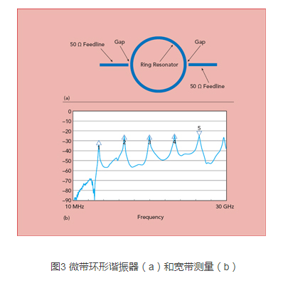
Figure 3b is the S21 response of a microstrip ring resonator based on a 10 mil thick board material, where Dk = 3.48. The approximate calculation of Dk is given by
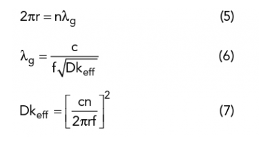
Although approximate, these formulas are useful for determining the initial Dk value. A more accurate Dk can be obtained using an electromagnetic (EM) field solver and a precise resonator circuit size.
The use of loosely coupled resonators to measure Dk and Df minimizes resonator loading effects. Making the insertion loss at the resonance peak less than 20 dB is considered loose coupling. In some cases, the resonance peak may not be measured due to the extremely weak coupling. This usually occurs on thinner thickness resonant circuits, which are commonly used in millimeter wave applications because the higher the frequency, the shorter the wavelength and the smaller the circuit size.
Millimeter wave test method
Although there are many Dk test methods, only some are applicable to millimeter wave frequencies, and none of them have been identified as industry standards. The following two methods are relatively accurate and highly reproducible in millimeter wave testing.
Differential phase length method
The microstrip line differential phase length method has been used for many years. This is a transmission line test method that measures the phase of two circuits with only physical lengths (see Figure 4). In order to avoid any changes in the material properties of the board, the design of the test circuit is as close together as possible on the material to be tested (MUT). These circuits are 50Ω different lengths of microstrip transmission lines, and the signal feed is in the form of a grounded coplanar waveguide (GCPW). At millimeter wave frequencies, the GCPW signal feed mode is very important because the design of the feed can have a significant impact on return loss. Termination of non-welded connectors should also be used to allow good contact between the coaxial connector and the test circuit without soldering. On the other hand, the same connector can be used for two different circuit tests. This minimizes the effect of the connector on the measurement results. For consistency, the same connector should always correspond to the same port of the Vector Network Analyzer (VNA). For example, if connector A is connected to port 1 of the VNA and connector B is connected to port 2 to test a shorter circuit, this should also be the case when testing longer circuits.

The phase subtraction of the long and short-circuit circuits also reduces the effects of the connector and signal feed area. If the return loss of both circuits is good and the connectors have a uniform orientation, most of the effects of the connector can be minimized. When the differential phase length method is used at millimeter wave frequency, the return loss is better than 15 dB below 60 GHz, and 60 GHz to 110 GHz is better than 12 dB.
The Dk extraction equation for the microstrip differential phase length method is based on the microstrip line phase response equation for circuits with different physical lengths:
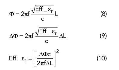
Where c is the speed of light in free space, f is the frequency of the S21 phase angle, ΔL is the difference in the physical length of the two circuits, and ΔΦ is the phase difference between the long and short line circuits.
The test method consists of a few simple steps:
Measure the S21 phase angle of a long and short line circuit at a given frequency.
Use the formula to determine the effective Dk.
Test the exact circuit size of the circuit, determine the initial Dk of the material and enter the EM field solver.
Use the software to generate a valid Dk value for the simulation. Change Dk in the solver until the effective Dk of the measured material at the same frequency matches the effective Dk of the simulation.
By increasing the frequency to the millimeter wave and repeating this process, the determined Dk value at the millimeter wave frequency can be obtained.
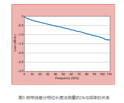
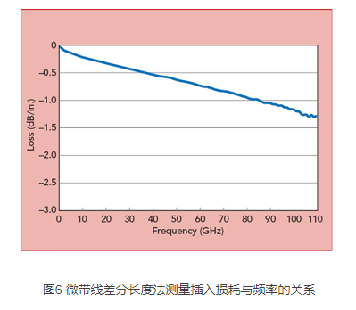
Figure 5 shows the variation of Dk versus frequency for a 5 mil RO3003G2TM board material using the microstrip line differential phase length method. The curve was obtained using the Dk calculation tool developed by Rogers. This data reflects the tendency for Dk to decrease as frequency increases. At lower frequencies, Dk varies greatly with frequency; however, Dk from 10 to 110 GHz varies little with frequency. This curve reflects a material with low loss and the use of smooth rolled copper, and materials with high loss and/or higher copper surface roughness exhibit a large negative slope with respect to frequency variation in Dk. Using this test method, it is also possible to obtain the insertion loss of the circuit of the material to be tested (MUT) by the S21 loss value of the long and short lines at each frequency (see Fig. 6).
The ring resonator method is another method for millimeter wave characterization. Although the ring resonator is usually used below 10 GHz, it has an appropriate processing accuracy and can be effectively used at a millimeter wave frequency. Machining accuracy is important because the effects of circuit size and dimensional tolerances are more pronounced in millimeter waves, and any variation reduces accuracy. Most millimeter-wave ring resonators are very thin (usually 5 mils) and the gap between the feeder and the resonator ring is small. The thickness of the ring resonator, the thickness of the copper plating of the line, and the change in the size of the gap all have an effect on it, thereby affecting the resonant frequency.
A circuit with thicker copper exhibits a lower Dk when comparing two circuits using the same board material but different copper thicknesses. Again, the resonant frequencies of the two circuits will be different, although they use the same board material and test methods. Figure 7 is an example of such a variation in the thickness of the final plated surface of the circuit resulting in a calculated Dk difference for the same material. Whether the surface treatment is electroless gold plating (ENIG) or other coated surfaces, the effect is similar.
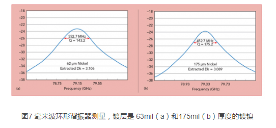
In addition to these processing problems, conductor width variations, etch coupling gap variations, trapezoidal effects, and substrate thickness variations can have similar effects. If all these changes are taken into account when testing Dk with a ring resonator, a single ring resonator measurement can yield the correct Dk value. However, many tests often use the nominal circuit size to test the calculated Dk, so it is not necessarily correct. Moreover, the lower frequencies are tested, and these effects do not significantly affect the Dk accuracy as the millimeter wave frequency.
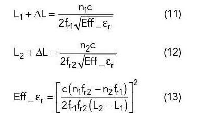
Another important variable in the use of ring resonators in the millimeter wave band is the coupling gap as a function of frequency. Typically, a ring resonator is evaluated with a number of different resonance points, and the coupling gap typically has a significant frequency difference with different resonance points. Therefore, the variation of the coupling gap may be an important source of error. To overcome this problem, a differential circumference method can be used. The two ring resonators used in this method are basically the same except for the circumference, and are integer multiples of each other (see Fig. 8). For two ring resonators, the higher order resonance points have a common resonant frequency in the Dk test. Since the feed line and the gap are the same, the influence of the coupling gap is reduced - theoretically eliminated - which makes the measured Dk more accurate. The formula for calculating Dk is as follows:
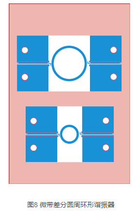
The ring resonator in Figure 8 is a microstrip structure, and the feed line is tightly coupled to the GCPW to avoid feeder resonance at the open end, avoiding interference with the resonant peak of the ring resonator. Usually if the feeders are open, they will have their own resonance. The only way to avoid this is to make the feeder shorter or use a tightly coupled GCPW feeder. Since the differential circumferential ring resonator method still yields the effective Dk of the circuit, accurate circuit size measurements are still required and the field solver is used to obtain the material Dk.
in conclusion
The millimeter wave test methods discussed here are all circuit based. There are many other test methods, such as raw material based test methods. But most methods test the material Dk of the x-y plane instead of the z-axis (thickness) Dk. Circuit designers use the z-axis Dk more often, but for some applications where the material xy plane Dk value is required, the free-space test method, the separation cylindrical resonator test method, and the waveguide perturbation test method are all The test method of the xy plane.
It has also been proposed to use a clamped wide-side coupled stripline resonator test method for determining the board material Dk at a millimeter wave frequency. However, this method is only effective for a small range of materials to be tested (MUT) and is not suitable for large-volume testing. Therefore, the test methods for raw materials that can be used for millimeter wave frequencies are still being studied.
Categories
Latest News
Contact Us
Contact: Ms Tracy
Phone: 0086 18682010757
Tel: 0086 18682010757
Add: Building9,Xinyuan Industrial Park,Tangwei,Fuyong,Baoan,Shenzhen,China
 Tracy
Tracy