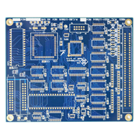
Fr4 PCB

Standard PCB thickness 4 layer FR4 Circuit Board
- fr4 pcb
- 4 layer pcb
- thick pcb
- multilayer pcb
- Product description: Standard PCB thickness 4 layer PCB thickness standard standard pcb thickness chart standard pcb thickness 2 layer What is the standard thickness of a copper layer on a pcb pcb thickness tolerance
Standard PCB thickness 4 layer FR4 Circuit Board
Material:ShengyiFR4
Layers:4
Solder mask:Green
PCB size:9*8CM
Copper:1OZ
Thickness:2.6mm
Surface finish:HASL
1,Standard ONESEINE PCB Thickness
The typical PCB thickness is 0.063inches or 1.57mm; it is a standardized level defined from the past. That is because, during the plywood industry, 0.063" was the thickness of the plywood sheets used as substrates for electronic devices, which included PCBs.
When multiple layer PCBs started developing, the thickness of the connectors between the boards had to match. Therefore, the level of consistency became a significant variable, and there was a requirement for a standard deck of the copper used as layers on the plate edges. In turn, 0.063" became the Standard PCB Thickness.
Nevertheless, there is a broad thickness range of 0.008 inches to 0.240 inches, between which you can choose depending on the application or usage area. It is, therefore, essential that you communicate requirements for the appropriate PCB thickness size.
2,What If I Want a Custom Thickness?
Sheets or panels used for manufacturing PCBs are easily available in the market. There are various customization options that offer designs and thicknesses as per your specifications and needs. You can pick the thickness range from 0.2mm to 6.3mm in millimeter increments of a hundredth. Read further to find out factors that must be supervised while opting for a customised PCB board thickness.
Factors to keep in mind for Custom PCB Thickness
1) Turnaround time: Generally, the expected turnaround time to receive a customized PCB layer thickness is more due to the uncommon thickness specifications. This will impact your delivery schedule and development timing.
2) CM’s equipment capabilities: If you do not want to compromise in your design and model, be careful while choosing your CM. If your CM has limited options of equipment to manufacture and design the typical PCB thickness you are looking for, you will have to compromise and modify your PCB layout.
3) Additional costs: Customization costs are generally higher due to the additional details and expectations. The use of specific material, design, and adhering to a detailed set of instructions amounts to additional manufacturing costs than usual prices.
Using customized thickness can increase the design appeal and yield, providing it an exclusive performance and value. However, using multiple layers can be very costly due to extra processing, manufacturing steps, and materials.
With a perfect manufacturing partner, the desired thickness can be achieved smoothly. The first step to customization is generally determining common core prepreg thickness and combining it in a perfect sequence with copper plating, copper foil, and solder mask.
We, at Absolute Electronics, take care of your needs with high-quality, accurate prototypes. We can cater to all your standard and customization needs with good designs and intent. Few highlights of our Custom PCB Manufacturing Service:
Accurate quote within 24 hours
The entire turnkey process performed within or less than three days
Reduced procurement time
Dedicated and committed Quality Certification
High PCB quality
Automated Optical Inspection
3,Factors That Impact PCB Thickness
While it is important to know industry standard thicknesses, many factors may necessitate a custom board. Depending on these design and manufacturing factors, your board may need to be a non-standard thickness. Two main groups of factors impact PCB thickness — design factors and manufacturing factors. We cover these factors in more detail below and will help you determine how to choose a PCB thickness for your project.
Design Factors That Impact PCB Thickness FROM oneseine
Design factors are considered during the PCB design phase. These factors mostly focus on the functionality and purpose of the board, rather than practical considerations necessitated during manufacture, though manufacturing factors hold equal weight. Some of the most important design factors that impact PCB thickness include the following:
1. Size, Weight and Flexibility
Thinner boards are lighter and more flexible than their thicker counterparts but will break more easily due to brittleness. While flex PCBs must be thin to achieve their flexibility, applications that do not require flexibility may benefit from a slightly thicker board for the sake of structural integrity. However, while thicker boards are more rugged, they also carry more weight and take up more space within a device. Both of these features may pose a problem for lightweight applications or devices with limited spatial capacity. The final application of the PCB determines these factors, which must be some of the first parameters to define before beginning PCB design.
2. Copper Thickness
Copper thickness plays a role in the overall thickness of the PCB. The thickness of the copper layer used usually depends on the current that needs to pass through the PCB. Standard copper thickness is roughly 1.4 to 2.8 mils (1 to 2 oz), but this thickness is adjusted according to the unique requirements of the board. The thicker the copper, the thicker the board and the more expensive the board will be due to material needs and processing challenges.
3. Board Materials
The operation and lifetime of a PCB depend on the choice of materials, but these choices also impact board thickness. Typical board fabrication consists of the substrate, laminate, solder mask and silkscreen. Of these, the laminate and substrate are the most important materials for consideration, as they provide the structure of the board and greatly impact overall thickness. The substrate may consist of paper and epoxy resin, glass weave or ceramic depending on the necessary dielectric constant. Laminates, on the other hand, consist of thermoset resin and either paper or cloth layers. Both laminates and substrates come in many options that determine the thermal, mechanical and electrical properties of a circuit board, but also determine the board’s overall thickness.
Categories
Latest News
Contact Us
Contact: Ms Tracy
Phone: 0086 18682010757
Tel: 0086 18682010757
Add: Building9,Xinyuan Industrial Park,Tangwei,Fuyong,Baoan,Shenzhen,China
 Tracy
Tracy