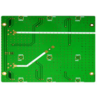
Printed Circuit Boards
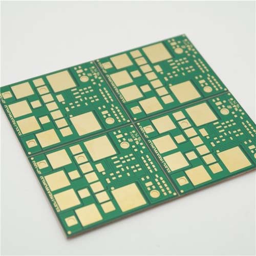
Heavy copper PCB Circuit Boards manufacturing process
- printed circuit boards
- Heavy copper PCB
- fr4 pcb
- High tg pcb
- Product description: Heavy copper PCB Circuit Boards manufacturing process
Heavy copper PCB Circuit Boards manufacturing process:
What is a heavy copper pcb circuit board?
Usually the conventional double-sided circuit board generally requires copper thickness of 10 / Z, and multi-layer circuit board is generally the inner layer 0.50 / Z, the outer layer 10 / Z,
There is also the inner layer due to impedance adjustment of the inner layer of copper thickness,so more than 10 / Z of copper thickness we can be regarded as thick copper circuit board
Heavy copper circuit board main control difficulty as below:
Thick copper circuit board is the main control point of its line width from the thicker copper corresponding to the line width from the greater the requirements, or very easy to etch.
In addition, as part of the product requirements of copper plate is not up to the need for board electricity, likely to cause uneven copper surface. So the process requires high, difficult to purchase circuit board.
The benefits of heavy copper circuit board:
The thicker the copper plate, the better the heat dissipation of the product.
The thicker the copper can carry the greater the current.
Copper thicker copper circuit board, the better the stability of the product.
The thicker the circuit board copper, the longer the product life.
Why use heavy copper pcb circuit board?
Due to the need to meet the application of special products and end-product environment
Long-term stability of the operation, so some special industries need to use the circuit board thick copper circuit board technology.
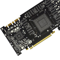
Heavy copper pcb is mainly used in those areas:
Thick copper circuit board is mainly used
In the field of transportation (such as automotive electronics, rail traffic signal control),
medical instruments,
Aerospace industry and industrial control and other fields.
The capacity of PCB manufacturers?
At present the general PCB manufacturer control the thickness of copper are 1.5 or 2 0Z,
As I know ONESEINE TECHNOLOGY company currently controls copper thickness can reach 210 um, that is 60Z.
Heavy copper PCB manufacturing process:
Thick copper main purpose is to ensure that the hole has a enough thick copper coating to ensure that the resistance value within the process requirements. As the insert is a fixed position and to ensure that the connection strength; as surface-mount devices, some holes only as a through-hole, play conductive on both two side .
(A) inspection items
1. The main inspection is metal hole quality , should ensure there are no extra material, burr, black hole, hole, etc in the hole.
2. Check the substrate surface if have dirty and unwanted residue;
3. Check the substrate number, drawing number, process documentation and process description;
4. Find out the location of hanging equipment, installation requirements and plating tank can bear the plating area;
5. Plating area and process parameters must be right, to ensure the stability&feasibility of the plating process parameters.
6. Clean-up and preparation for conductive parts, power on first and so that the solution assumes an activated state
7. Check the touch position and voltage, current fluctuation range.
Line Space & Line Width on heavy copper PCB
|
Copper |
Min line width |
Min line space |
|
2OZ |
0.20mm |
0.23mm |
|
3OZ |
0.25mm |
0.28mm |
|
4OZ |
0.35mm |
0.33mm |
|
5OZ |
0.45mm |
0.38mm |
|
6OZ |
0.60mm |
0.43mm |
|
7OZ |
0.70mm |
0.48mm |
|
8OZ |
0.80mm |
0.53mm |
|
9OZ |
0.90mm |
0.58mm |
|
10OZ |
1.00mm |
0.63mm
|
|
11OZ |
1.10mm |
|
|
12OZ |
1.20mm |
|
|
13OZ |
1.30mm |
|
|
14OZ |
1.40mm |
|
|
15OZ |
1.50mm |
|
|
16OZ |
1.60mm |
|
|
17OZ |
1.70mm |
|
|
18OZ |
1.80mm |
|
|
19OZ |
1.90mm |
|
|
20OZ |
2.00mm |
Categories
Latest News
Contact Us
Contact: Ms Tracy
Phone: 0086 18682010757
Tel: 0086 18682010757
Add: BludingA,Shixiaganglian Industrial Park,Shajing,Baoan,Shenzhen,China
 Tracy
Tracy Tracy
Tracy